In the previous post, I described a circuit design for a TDCS controller I’m developing. Because I’m working almost exclusively with surface mount components, I can’t really breadboard the circuit. The best option I have is to build a circuit board and use that for testing. Conceptually, I could send the board out to a fab shop and have them produce one. However, doing a 1-off build, especially when the design hasn’t been proven, is expensive, risky, and takes a while. Because I’m impatient and like to do things myself, I make my own. In this post, I’ll describe the process I use for making my own boards.
If you happen to be interested in trying this yourself, you’ll need a few things:
- A circuit board layout
- Dry-film photo resist
- Double-sided copper-clad circuit board(s)
- 300-400 grit sandpaper
- Printable transparencies (ink-jet printable in my case)
- A good quality printer
- A laminator
- A laminator pouch that has been through the laminator
- Latex gloves
- Washing soda (sodium carbonate)
- Copper Etchant (I use ferric chloride)
- UV curable solder mask
- A UV light source (a black-light works well)
- A rotary tool (Dremel) and carbide bits
- A hacksaw to cut out the finished board
- Soldering Iron and solder
I make my boards by laminating bare copper clad board with dry film photoresist. I then print the pattern negative onto an inkjet printable transparency to use as a photomask while exposing the photoresist. To make the mask, I use Eagle CAD to build the board layout as part of the circuit design. However, I don’t like the way Eagle exports the graphics. I turn off all the layers but pads, vias, and either top or bottom layers and export the result as a PNG at 1200 dpi. However, the exported graphic isn’t quite ready for exposing a board. First, it isn’t black and white. In order for the photomask to work right, it needs to be either transparent (white) or black. Second, with the latest version of Eagle the signal names are printed on the traces and need to go away. Finally, the drill-holes are almost filled, and it’s much easier to hand-drill if the etched copper acts as a sort of pilot hole to guide the drill.
Using Gimp and a round brush I erase (paint over in black) anything that blocks the drill holes. Then I use the threshold tool to turn it to black and white. Once that is done, I mirror-image the bottom layer and add any graphics (like my logo) and text I want or have room for. In the end, anything black in the image will be areas where the copper is etched away.
To build the mask for curing the solder mask, I turn off all the layers in eagle except either the tStop or bStop layers, change the fill pattern to a solid color, and export it using the same settings as the board layout. Using Gimp, I use the threshold tool to make it black and white, then invert it so that the pad areas are black (black areas won’t cure and can be wiped off when the mask is applied).
Printable transparencies are kind of expensive, so I try to cram as much onto each one as I can. To do this, I use Scribus to lay out a full page that includes all the masks I need. A calculator and the properties dialog box are handy to make sure the relative geometries of tiled masks are the same. Finally, I use Scribus to export the result as a PDF for printing. Generally, I’ll print out a sheet on copy paper and make sure things line up, and that device footprints match the components I have on-hand. Make sure you don’t have “shrink to fit” selected on the printing options, and when you print the actual mask, set the print quality to maximum and resolution to at least 600dpi.

To laminate the dry-film photoresist onto the copper-clad board, I start by using 320-grit sandpaper to sand off oxidation and contamination from the board. I’ve tried using brillo pads and cleanser, but have had issues with the film not adhering strong enough and pulling loose at inopportune times. Once the copper has been sanded bright, I clean it off with acetone to make sure I didn’t leave any oils on it. I also wear cheap latex gloves from Harbor Freight any time I handle the board to make sure I don’t get skin oils on it.
Once the board is clean, I cut a piece of film about 1″ wider and longer than the board I want to laminate. I also cut a piece of card stock about 2″ longer and wider than the board. The dry-film photoresist is protected by a thin sheet of plastic on both the top and bottom, and one of these protective sheets needs to be removed in order for the film to work. To separate it, I sandwich the corner edge of the film between two pieces of scotch tape (sticky-side to sticky-side) and peel the tape apart. One side of the protective film will peel away (usually the inner side based on the way it wants to curve). If it doesn’t, try again, maybe on a different corner.

I then tape the top-edge of the film face-down (protective layer up) on the card stock. I align the board underneath the film and feed the film into a hot laminator taped-end first. The laminator will grab the paper and begin pulling it through. Gently lift up on the film to keep gentle tension on it and avoid bubbles or wrinkles as it feeds into the laminator. Once it’s been through, I usually run it through two or three more times just to make sure it’s good and stuck. At this point, the film around the edge of the board is laminated to the cardstock, so I cut around the board with a utility knife to get the board free. Then, I turn the board over and repeat the process for the bottom.

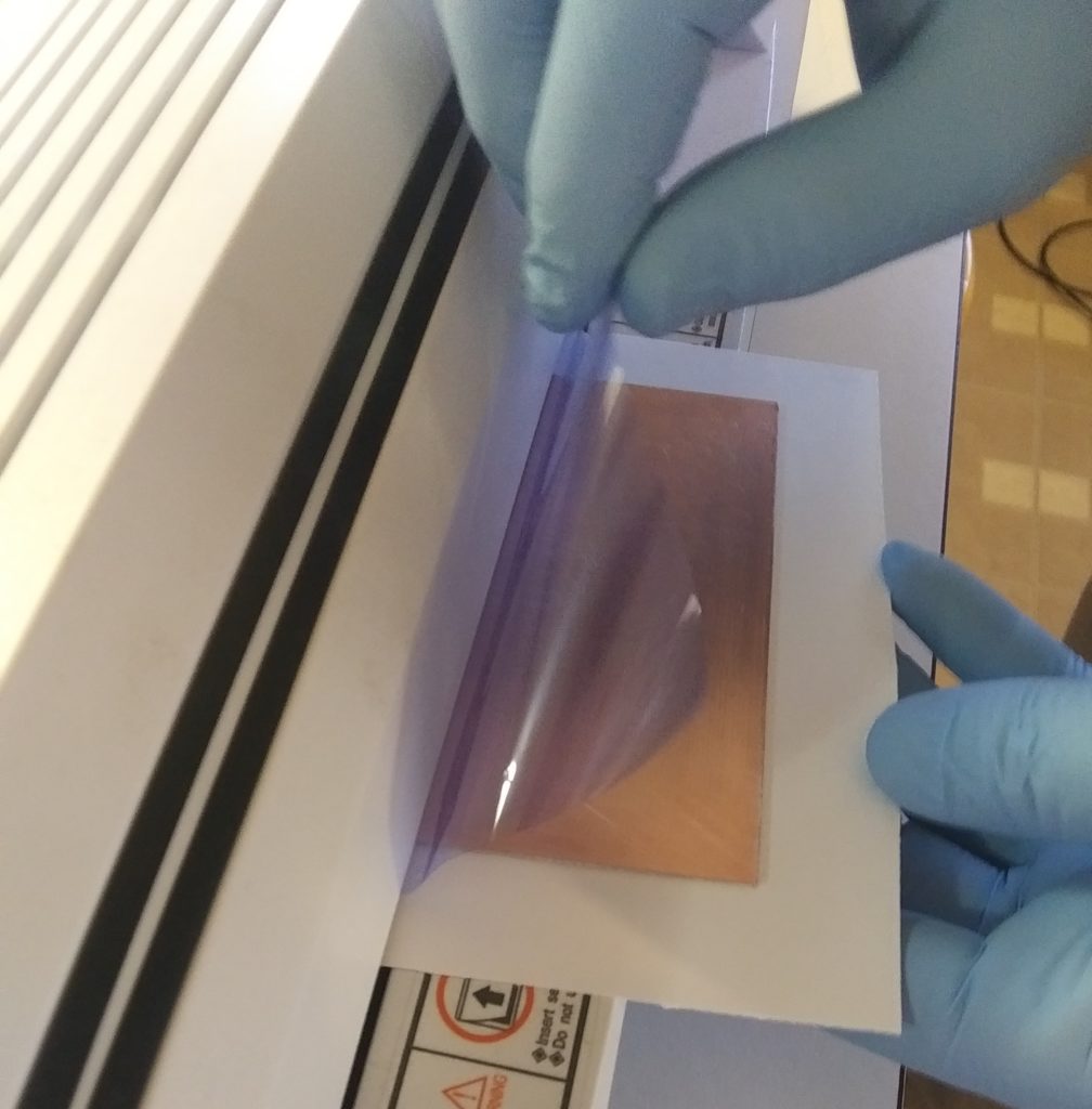
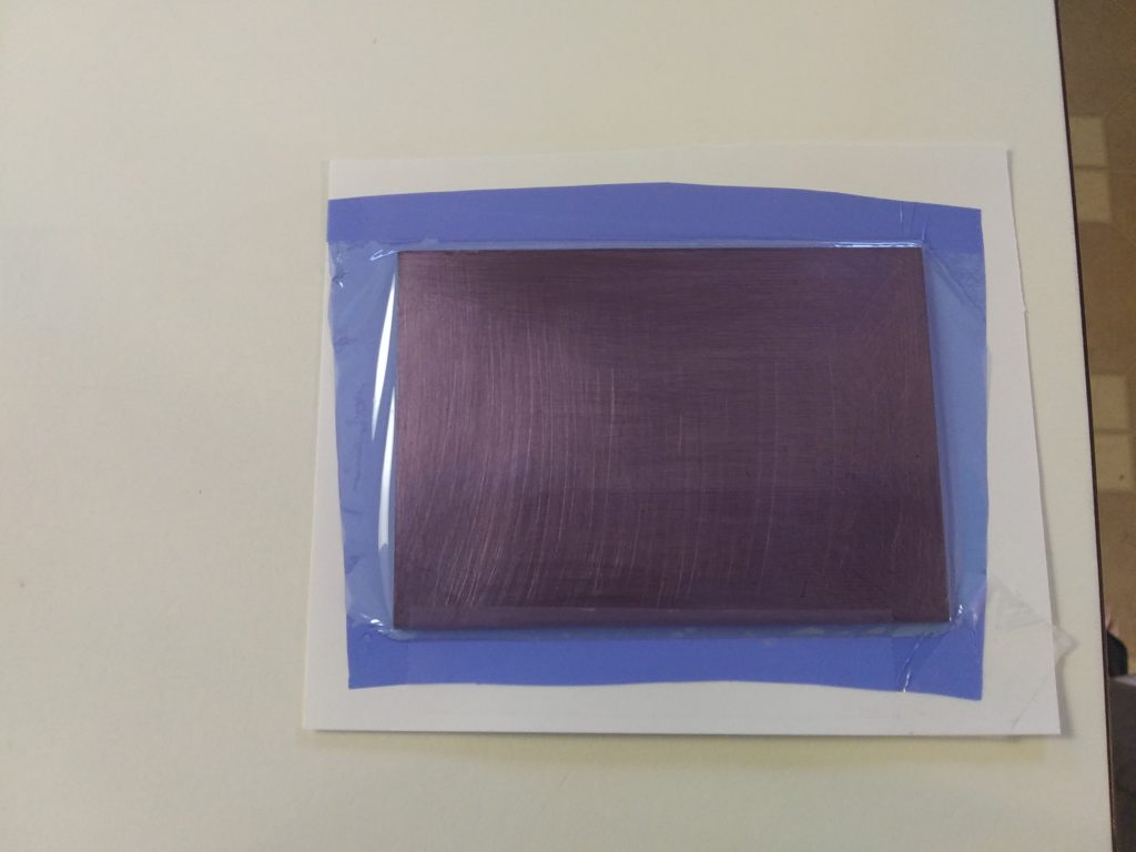
To align the top and bottom masks I cut them out, leaving about a 1/2″ margin around the pattern, and use a piece of left-over circuit board to act as a spacer between them. I tape one of the masks to the piece of board, then flip it over and tape the other mask down so that it’s aligned. It isn’t exact, but it’s about as good a way as I’ve found for consistency. When I’m ready to expose the board being etched, I slide it between the masks, and sandwich it between two pieces of glass that I took out of a thrift-store picture frame. Rubber bands, binder clips, or clothespins work pretty well to keep it all together (you have to flip it over without messing with the alignment, so it’s important to get at least some tension on it).
I’ve seen lots of folks on the web double-layering their masks to get stronger contrast, but in my experience this is totally unnecessary, and can make it really hard to work with small features. It’s almost impossible to get them exactly aligned, and variances in the printer can make it absolutely impossible. Using a single layer mask I’ve reliably made boards with traces down to about 10mils (1/100th of an inch) that turned out crisp. However, I do prefer to keep all the clearances and trace widths 15 mils or larger just to make it easier on myself.

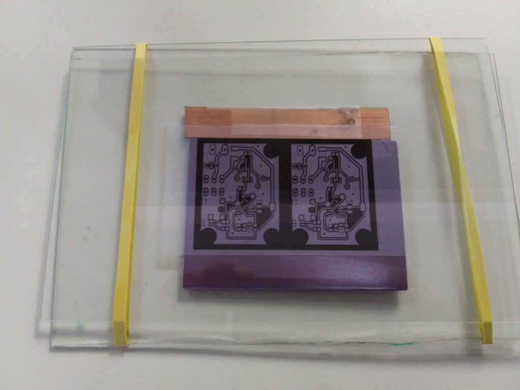
The photoresist is sensitive to UV light (and to a lesser degree it’s sensitive to the blue-end of visible). Some people have had success using fluorescent lights a few inches above the board, but that didn’t work particularly well for me. Others use sunlight, but I like to be able to work when it’s dark or cloudy outside, and the UV from the sun can vary widely based on time of day and cloud conditions. My solution was a 13W black-light LED bulb I bought at Lowes or Home Depot. I rigged up a fixture that holds it about 4 inches above the board. In this configuration, a 5 minute exposure is about right. Your mileage may vary, and you’ll likely have to experiment with different exposure times to get consistent results. Take good notes and it won’t take long to make beautiful boards.


To develop the photoresist, carefully peel off the protective plastic. Use tape on the corner and lift up if you can’t get it with your fingers. Be very careful and gentle, pulling the plastic outward and upward to avoid tearing the film. This is one point where you find out if your board was totally clean and if the laminator was hot enough. If the photoresist starts to peel off, clean it off with acetone or a long bath in hot water and washing soda and start over. Assuming the plastic comes off cleanly, drop the board in some luke-warm water with washing soda* dissolved in it. It isn’t critical how much. I usually use about a teaspoon or two per cup of water. If the water is too hot, you may end up washing away both the developed and undeveloped portions and have to start over
*you can find washing soda in the laundry isle of most grocery stores, or you can make your own by heating baking soda in the oven at 350F for half an hour or so.

Gently agitate the board, and lightly rub it with a paintbrush or soft toothbrush (I used cheap acid brushes from the plubming section at Harbor Freight). The unexposed areas will soften and gradually wash away. Keep going until all the copper you want to etch away is completely exposed. You can patch up areas that are accidentally exposed by drawing over them with a sharpie after the board has dried off and before etching, but I prefer to just re-do the exposure since it turns out much neater that way. When all the copper you want etched away is exposed, rinse the board in cold water to stop the developer from eating away the film you want to keep. Let the board dry before you try to re-touch any copper that got accidentally exposed.

At this point, the board is ready to etch. At the moment, I’m using Ferric Chloride etchant, but you can find tutorials on the web for making your own etchant from hydrogen peroxide and hydrochloric acid (muriatic acid for cleaning swimming pools) you can buy at WalMart. Pour some etchant into a non-reactive container and swish the board around. The board will etch faster if the etchant is warm. Also be careful with FeCl… it indelibly stains almost everything it touches, especially clothes, skin and counter tops. Definitely use gloves, and lay down some paper towels or cardboard to protect your work surface. Check the board every few seconds. Quit when all the exposed copper has been eaten away and rinse the board with plenty of warm water. Don’t dispose of this stuff down the drain, the copper in it will kill aquatic life. I’m currently looking for a good chemist to show me how to precipitate the copper out of the solution so I can neutralize the remainder and flush it down the drain. Until then, I pour the etchant back in its original container and keep it.


Depending on how impatient you are, and what you have available to you, a short soak in acetone will quickly loosen up the photoresist. I don’t really like working with harsh organic solvents like acetone, so I usually just drop the board into a solution of hot water and washing soda and leave it overnight.

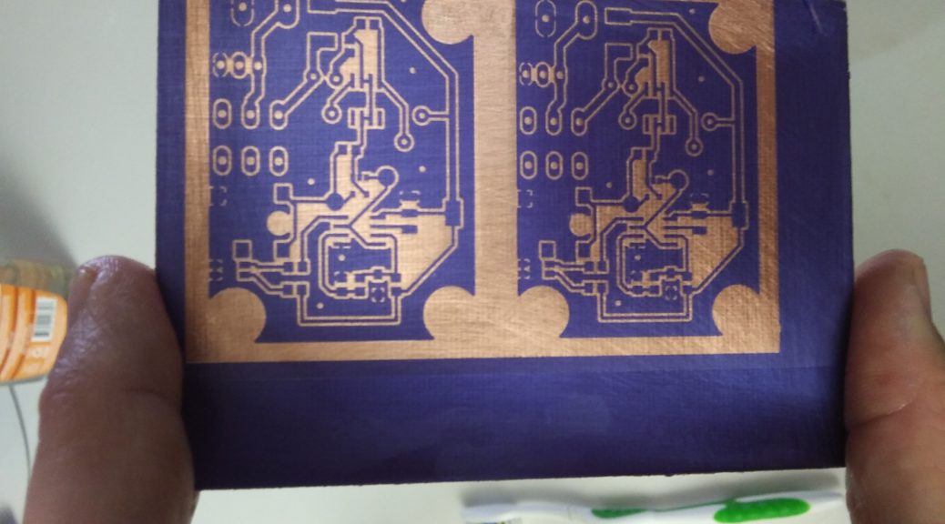
If you are working only with through-hole components, you can stop after the film has come off, drill the holes with a dremmel or drill press, and start building the board. However, I prefer surface mount components, and those are much easier to work with if you apply solder mask. Besides, solder mask makes the board look better (even if you screw it up a little like I tend to). The soldermask I use is a UV curable epoxy paint that is heat resistant enough that it won’t blister when you solder components to the board. It’s available online from places like ebay and Amazon. To make it work, you need a thin layer, so I squeeze a small amount of the paint onto the board, then squeegee it under a sheet of transparent plastic (I use a laminator pouch that has been through the laninator). The biggest problem I’ve had is getting the paint too thick so the UV light doesn’t penetrate far enough to cure the deeper layers. Spread it out THIN. I’ve also found that taping one edge of the transparency to a piece of cardstock will help minimize the sheet or board slipping with respect to each other (not shown in the pictures).


Once you have a thin layer of paint, expose it using the same setup as was used to expose the photoresist. Five minutes seems about right with my setup, but you’ll likely need to experiment on some scrap boards to get it right. Don’t experiment on large areas. There is no way to peel off the stuff once it’s cured. It’s tough as nails. After exposing it, lift the clear plastic and wipe the board with a clean paper towel to expose the component pads and vias. Wipe it thoroughly. I’ve used an acetone dampened paper towel before, but you run the risk of blistering incompletely cured paint. Once the pads are clean and bright copper, put the board back under the light for another ten or so minutes to make sure it’s fully cured.

After wiping off the uncured paint, I put it back under the light for 10 or so minutes to make sure it’s good and cured. Once the paint is dry, I use a dremmel with bits I got on amazon to drill out the vias and through-hole components. Finally, I cut the board out. A hack-saw works okay, and band-saw works better (I don’t have one of those yet). A dremmel with a cut-off wheel will work in a pinch (what I used here).

At this point, the board is ready to build up. Solder on the components according to the schematic and fire it up to test. Soldering surface mount components is an art form of its own, but the short version involves using plenty of flux paste, dental picks to hold things in place, and solder wick to suck up extra solder when you get too much. Be careful not to overheat the components. If things aren’t going as planed, stop and let things cool off.
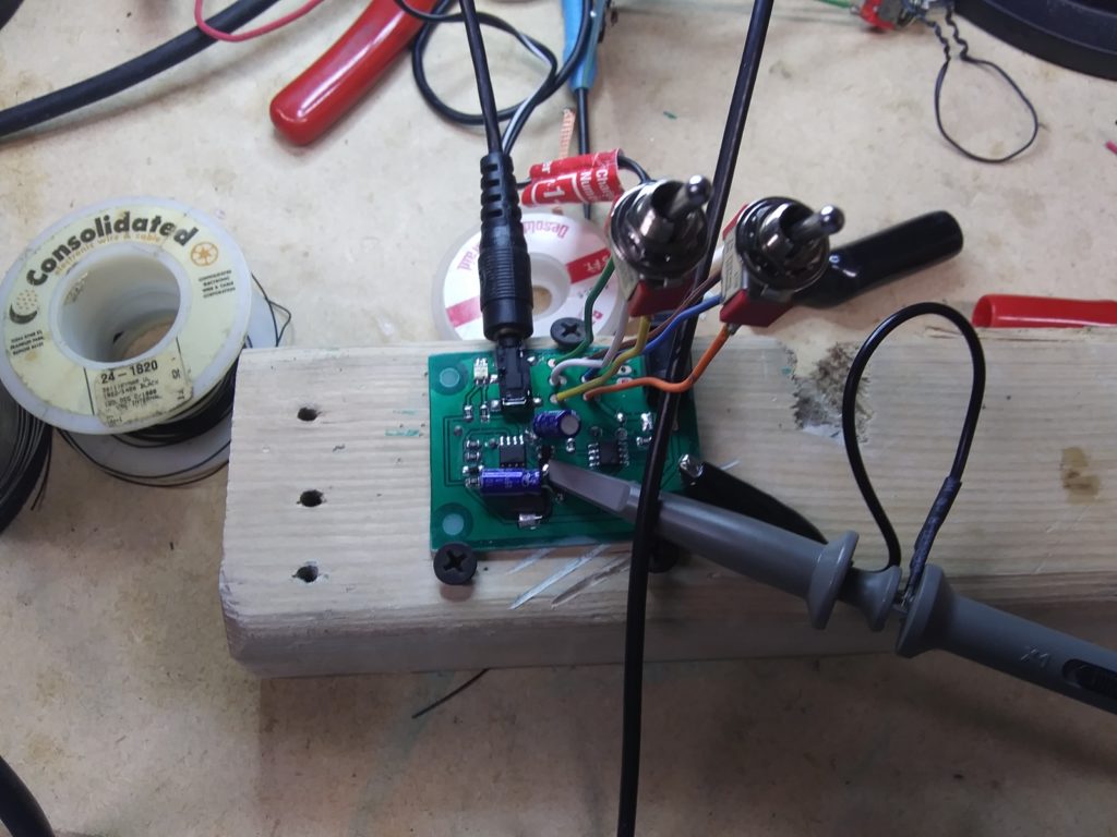
There you have it. That’s how I build prototype circuit boards. Now it’s time to test it.
3 thoughts on “TDCS Controller Step 2 – Building The Circuit Board”